Semiconductor Cleaning Process Optimization

Matsushima Measure Tech
Optimizing the cleaning process in semiconductor manufacturing has become a crucial challenge to ensure device performance and reliability. Recent research shows that advanced techniques combining wet and dry cleaning, as well as innovative methods such as megasonic cleaning, can improve cleaning efficiency and reduce resource consumption.
The difference between wet and dry
Wet cleaning and dry cleaning in semiconductor manufacturing are important cleaning technologies, each with their own unique characteristics and applications.
Wet cleaning is the primary technology that accounts for over 90% of the cleaning steps in semiconductor manufacturing. This method uses liquid chemicals and ultrapure water in combination with physical techniques such as ultrasound/megasonics, heating and vacuum to remove contaminants from the wafer surface.1 The main objective is to remove particles, native oxides, organics, metal contamination, sacrificial layers, polishing residues, etc.
Common wet cleaning techniques include:
- RCA Cleaning: Uses a mixture of ammonia, hydrogen peroxide and water (APM) and hydrochloric acid, hydrogen peroxide and water (HPM) to remove organic matter and heavy metal ions.
- IMEC Cleaning : Uses ozone and diluted chemicals to conserve resources.
- Single Wafer Cleaning: Minimizes cross-contamination and surface damage, improving product yields and reducing costs.
Dry cleaning, on the other hand, does not use liquid chemicals but instead relies on gas-phase chemical techniques such as plasma cleaning, supercritical carbon dioxide cleaning, and beam cleaning. This technique excels at creating fine lines and geometric patterns due to its anisotropic etching properties.
The main features of dry cleaning are:
- Plasma cleaning : Inert gases are excited into a plasma state, which reacts with surface molecules to form volatile products.
- Beam cleaning: uses a fine beam of conductive cleaning agent to efficiently remove impurities by breaking the van der Waals bonds between atoms.
- Laser beam cleaning: effectively removes micrometer and sub-micrometer sized particles without damaging the silicon surface.
Dry cleaning is essential for logic and memory products, primarily at technology nodes below 28nm, but it faces challenges due to the potential for undesirable reactions with silicon surfaces from chemical vapors and the inability to completely remove all metallic contaminants.
Both technologies play complementary roles in semiconductor manufacturing, contributing to the miniaturization and high performance of devices. Selecting the appropriate cleaning method for each stage of the manufacturing process is essential to producing high-quality semiconductor devices.
Reducing Chemical Consumption Strategies
Reducing chemical usage and reducing environmental impact has become a key challenge in the semiconductor manufacturing industry.
To address this challenge, several innovative strategies have been developed.
- Adopting closed-loop chemical recycling systems : This allows manufacturers to reuse chemicals after a single use, reducing waste and making efficient use of resources.
- Introduction of new RCA cleaning technology: By integrating the conventional two-stage cleaning of SC-1 and SC-2 into one stage, the amount of chemicals used and the amount of waste liquid are significantly reduced.
- Development of technology to reduce organic wastewater : We are working to reduce the environmental impact by introducing new technologies that focus on reducing the amount of chemicals used and limiting the amount of wastewater.
These strategies are helping to make semiconductor manufacturing processes more efficient and sustainable, marking an important step toward achieving carbon neutrality across the industry.
Purpose and method of cleaning by process
The purpose of cleaning in semiconductor manufacturing processes and the type of cleaning solution used at each step are crucial to ensuring product quality and performance. The table below summarizes the purpose of cleaning in the main manufacturing processes and the cleaning solutions used.
| Process | Purpose of cleaning | Cleaning fluid used |
| Initial cleaning | Removal of organic and particulate contaminants | Deionized water, organic solvents (acetone, isopropyl alcohol) |
| Oxide film removal | Native oxide removal | Hydrofluoric Acid (HF), Buffered Oxide Etchant (BOE) |
| RCA cleaning (SC1) | Removal of organics, light metals and common contaminants | A mixture of ammonia water (NH₄OH), hydrogen peroxide (H₂O₂), and deionized water (APM) |
| RCA cleaning (SC2) | Removal of metal ion contaminants | A mixture of hydrochloric acid (HCl), hydrogen peroxide (H₂O₂), and deionized water (HPM) |
| Piranha Cleaning | Removal of organic residues and metal contaminants | Mixture of sulfuric acid (H₂SO₄) and hydrogen peroxide (H₂O₂) |
| Post-CMP cleaning | Removal of particulate deposits such as silica and ceria | Dedicated rinse aid (e.g. CLEANTHROUGH KS-7000 series) |
| Photoresist Removal | Photoresist and organic contaminant removal | Dedicated resist remover (e.g. CLEANTHROUGH KS-7000 series) |
| Final wash | Removal of residual chemicals and final surface preparation | Deionized water, isopropyl alcohol (IPA) vapor |
These cleaning processes effectively remove various contaminants from the surface of semiconductor wafers to ensure device performance and reliability. For example, RCA cleaning is a two-step process to remove organics and metal ions, and uses a combination of SC1 and SC2 to thoroughly clean the wafer surface.
Piranha cleaning is particularly effective at removing organic residues and rendering the wafer surface hydrophilic through its strong oxidizing action, while post-CMP cleaning uses specialized rinse chemicals to remove fine particulate deposits resulting from the polishing process.
Modern cleaning technologies aim to reduce the environmental impact and improve cleaning efficiency by using fewer chemicals while still providing more effective cleaning. For example , the development of advanced cleaning chemicals has enabled fewer cleaning cycles and simplified cleaning processes.
Proper selection and use of these cleaning processes and cleaning solutions is key to quality control and yield improvement in semiconductor manufacturing and is an essential element in the production of cutting-edge devices.
Proper storage of cleaning solutions
Proper storage of cleaning fluids in semiconductor manufacturing is crucial to ensure the efficiency and safety of the cleaning process. The table below summarizes the storage conditions and precautions for the major cleaning fluids.
| Cleaning solution | Storage conditions | Note |
| Sulfuric acid/hydrogen peroxide mixture (SPM) | Temperature: 10°C to 30°C, in a well-ventilated area | Stable for over 100 days, usable at high temperatures |
| RCA cleaning solution (SC1, SC2) | In an inert tank at approximately 80°C | Prepare immediately before use and use within 10 minutes |
| Hydrofluoric Acid (HF) | Dedicated acid-resistant container, cool and dark place | Store separately from other chemicals |
| Organic solvents (acetone, IPA) | Fireproof storage, well-ventilated area | Beware of flammability, keep away from heat sources |
| Ozone Water | Light-shielding container, low temperature environment | Decomposes quickly, so prepare immediately before use. |
Temperature control, ventilation and proper containers are essential for storing cleaning solutions. For example, SPM solution is a mixture of 31.25 cm³ water, 18.75 cm³ 98% sulfuric acid and 50 cm³ 35% hydrogen peroxide, and can be stored stable for over 100 days under proper conditions. On the other hand, RCA cleaning solution is recommended to be prepared just before use and used for a short time in an inert tank at high temperature. These proper storage methods will maximize the effectiveness of the cleaning solution and ensure its safety.
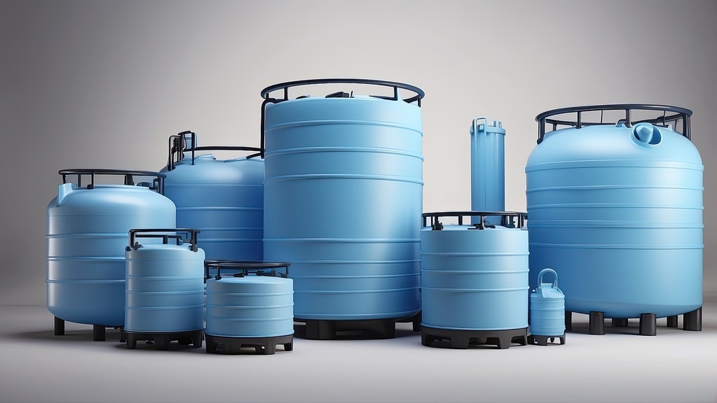
The Importance of Tank Management
Level monitoring of cleaning solution tanks in semiconductor manufacturing processes is essential to ensure efficient and safe operations.
Implementing the right monitoring system provides key benefits, including:
- Optimize chemical usage : Accurate knowledge of tank levels prevents overuse or shortage of cleaning fluids, ensuring efficient use of resources.
- Improved safety : Reduces the risk of tank overfilling and leakage, ensuring worker safety.
- Maintain process continuity: Prevent production line stoppages due to lack of cleaning fluid and increase productivity.
- Leverage real-time data: Remote monitoring enables faster decision-making and preventative maintenance.
These advantages contribute significantly to quality control and reduced environmental impact in semiconductor manufacturing, helping to realize sustainable production processes.
Types and features of level sensors
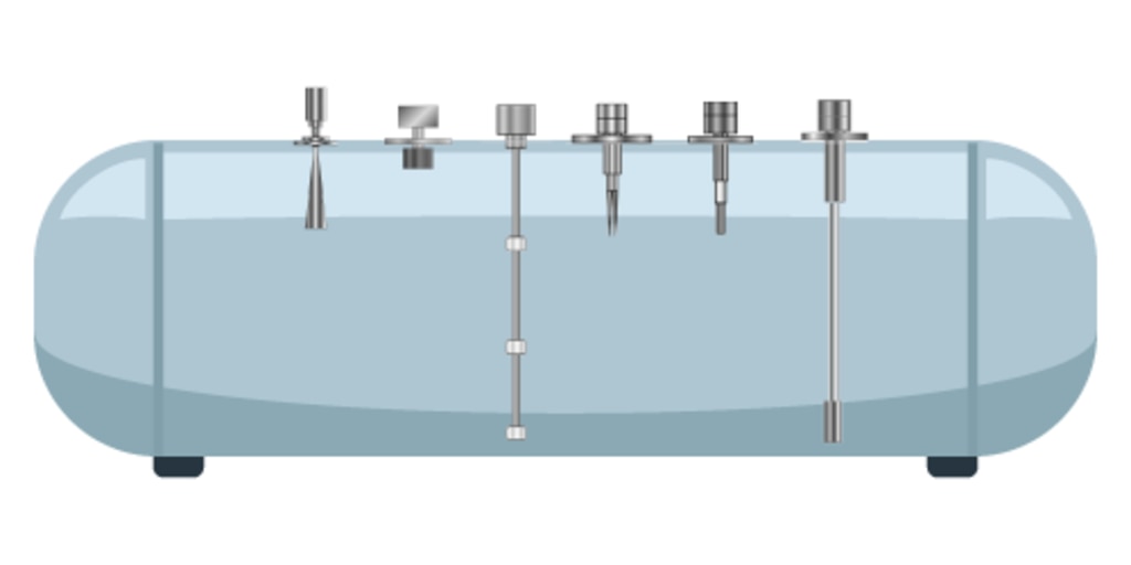
Various types of level sensors are used to manage cleaning solution tanks in semiconductor manufacturing processes. These sensors play a key role in accurately measuring the liquid level in the tanks to ensure an efficient cleaning process and safe operation. The table below summarizes the main level sensor types, their working principles and features.
| Sensor Type | Operating Principle | Features |
| Ultrasonic Sensor | Measures the reflection time of ultrasonic pulses | Non-contact, applicable to a variety of liquids |
| Capacitive Sensor | Detects changes in capacitance due to liquid level | Applicable to conductive and non-conductive liquids, high accuracy |
| Float Switch | The buoyancy of the liquid causes the float to move up and down, activating the switch. | Simple , reliable, low cost |
| Optical Sensor | Detects changes in light reflection and refraction due to the presence or absence of liquid | Non-contact, fast response, applicable to corrosive liquids |
| Radar Sensor | Measure the reflection time of microwaves | High accuracy, not easily affected by temperature, pressure or dust |
These sensors are used for appropriate applications according to their respective characteristics. For example, ultrasonic sensors are non-contact and can be used with a variety of liquids, making them suitable for monitoring highly corrosive cleaning liquid tanks. Meanwhile , optical sensors have a high-speed response and are effective for monitoring specific points such as detecting whether a tank is full or empty.

Commitment to sustainability
The semiconductor industry is taking a proactive approach towards sustainability and environmental protection.
Key strategies include:
- Reducing greenhouse gas emissions: Samsung has developed products that reduce carbon emissions by approximately 680,000 tons, and NVIDIA has increased its renewable energy usage to 76% by 2023-2024.
- Improved energy efficiency : Progress is being made in developing low-power chips and optimizing manufacturing processes to reduce energy usage.
- Water Stewardship: Intel has a goal of achieving net positive water usage by 2030.
- Waste Reduction: Intel is working to achieve zero waste by 2030 and will reuse and recycle 94% of its waste as of 2023.
- Developing green manufacturing technologies : The use of raw materials with low GWP (global warming potential) and the introduction of technologies to reduce fluorinated gas emissions are being promoted.
Through these efforts, the semiconductor industry aims to achieve sustainable growth while reducing its environmental impact.
Please feel free to ask us if you have any questions
or you want our support. ⇩⇩⇩
Please feel free to contact us if you have any inquiries.
Click here to download documents.


© Matsushima Measure Tech Co., Ltd.